
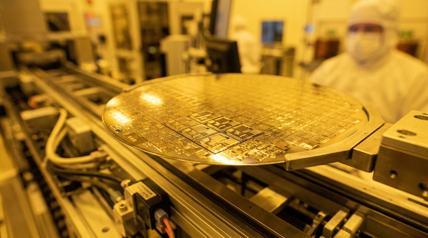
The semiconductor industry has reached a watershed moment. As artificial intelligence workloads demand exponential increases in compute capacity and energy efficiency, traditional Moore's Law scaling has faced physical limits. However, in mid-2026, researchers have officially broken through the angstrom barrier, ushering in the era of sub-1 nanometer (sub-1nm) silicon.
The 0.7 nm (7 Angstrom) Milestone
In a landmark development, IBM unveiled the world's first 0.7 nm chip architecture. Rather than relying on traditional two-dimensional planar or standard Gate-All-Around (GAA) designs, this breakthrough uses a revolutionary 3D "nanostack" architecture. By vertically stacking nanosheets, engineers can pack nearly 100 billion transistors onto a fingernail-sized piece of silicon.
This layout offers dramatic improvements in performance and efficiency:
- Performance Boost: Up to 50% higher computing speeds compared to the current 2 nm semiconductor nodes.
- Energy Reduction: Up to a 70% decrease in power usage for the same workload, solving one of the largest crises facing modern AI data centers.
- Thermal Efficiency: Optimized current flow controls leakage and thermal output, crucial for high-density mobile and edge computing devices.
Comparative Analysis: The Evolution of Chip Nodes
| Node / Size | Transistor Density (approx.) | Primary Architecture | Key Use Cases (2026) |
|---|---|---|---|
| 5 nm / 3 nm | ~150-220M / mm² | FinFET / Early GAA | Consumer smartphones, desktop CPUs |
| 2 nm | ~300M+ / mm² | Gate-All-Around (GAA) | Hyperscale cloud, flagship mobile chips |
| 0.7 nm (Sub-1nm) | ~1.5B+ / mm² | 3D Nanostack GAA | Next-gen LLM training, quantum-hybrid computing |
Overcoming the Physical Limits of Silicon
At the 0.7 nm scale, chips face quantum tunneling—where electrons literally leak through barriers, causing data corruption and massive heat. The 3D nanostack architecture tackles this by surrounding the channel on all four sides with a high-K dielectric material, ensuring precise electrical control. Additionally, 2026 manufacturing has matured the integration of backside power delivery, routing power lines beneath the silicon substrate rather than through top-level metal stacks. This reduces voltage drops and leaves more space on top for high-density data connections.
What This Means for AI and Cloud Infrastructure
As AI training workloads balloon, the carbon footprint of massive GPU clusters has become a bottleneck. By shifting to sub-1nm nodes, hyperscalers can host 3x the AI capacity within the same power grid envelope. For edge computing, this means consumer hardware can run large, complex agentic models directly on-device without needing internet connectivity or draining battery life.